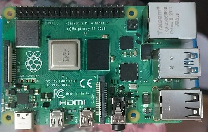
I unboxed my “new” Pi-4b and here’s a close-up view of it.
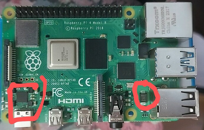
The thing that’s immediately apparent is the changes in the board’s layout, particularly with moving D1, (the reverse-voltage protection diode), to the other side of the PCB.
Viz.:
The thing that concerns me is that there isn’t a lot of “meat”, (fat circuit traces), between the power circuitry on the left, and the protection diode on the right. That, (to me), raises the issue of “what happens when a 3+ amp power supply is inadvertently connected backwards?” Without beefy traces, all I think you will see is, firstly fried traces, and then a fried PCB.
Of course this assumes some clod, (like me!), connects an unprotected, high-current supply to their Raspberry Pi. ![]()


